1 Chua’s oscillator
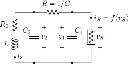
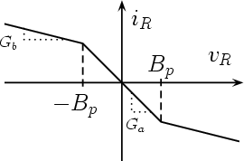
The Chua’s oscillator is shown in Fig. 1, together with a typical Chua’s diode characteristic. Note that for R0 = 0 we obtain the (classical) Chua’s circuit.
1.1 State equations
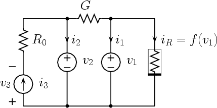
The circuit used to get the state equations of Chua’s oscillator is shown in Fig. 2, where each capacitor has been substituted by a voltage source and the inductor by a current source.
The state equations are obtained by computing the currents i1 and i2 through the two voltage sources and the voltage v3 across the current source and remembering that

The state equations are:
![dv 1
dt1- = C--[(v2- v1)G - f(v1)]
{ dv 11
--2- = ---[(v1- v2)G + i3]
dt C2
di3 = - 1-[v2 + R0i3]
dt L](chua-osc4x.gif)
with
![f (v1) = Gbv1 + 0.5(Ga - Gb)[| v1 + Bp |- |v1- Bp|]](chua-osc5x.gif)
1.2 Dimensionless state equations
Let us scale time, voltages, and currents by RC2, Bp, and BpG, respectively. Then let us assume as variables:

With these assumptions, we obtain the following dimensionless state equations:
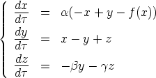
with

and with
![f(x) = m1x + 0.5(m0 - m1)[ |x + 1|- |x - 1 |] , m0 = GaR , m1 = GbR](chua-osc9x.gif)
Note that the case  = 0 corresponds to the (classical) Chua’s circuit.
1.3 Equilibrium points
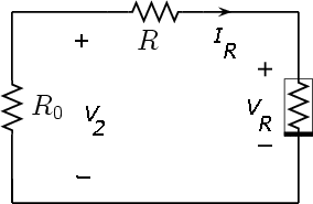
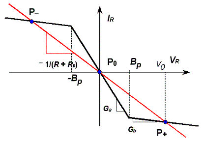
The equilibrium points are computed by setting to zero the derivatives in the state equations. That means that the capacitors are substituted by open circuits and the inductor by a short circuit, leading to the circuit of Fig. 3. Graphically, the equilibrium points are obtained by intersecting the "load line" of slope -1/(R + R0) with the Chua's diode characteristic.
|
|
2 Design of the Chua’s diode
In this Section we will design a resistive one-port with a piecewise linear characteristic, to be used in the realization of the Chua’s oscillator of Fig. 1. The operational amplifier is used as a basic element. Before giving any design formulas, let us briefly summarize the main properties of the ideal operational amplifier.
2.1 The ideal operational amplifier
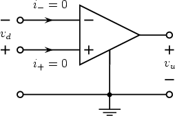
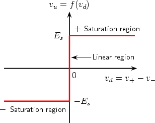
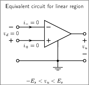
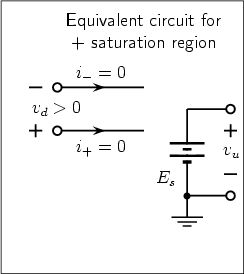
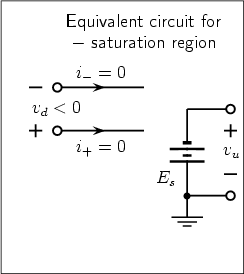
The symbol of the ideal operational amplifier (op-amp) and its transfer characteristic are shown in Fig. 4. The equivalent circuits for linear and saturation regions are shown in Fig. 5.
2.2 A locally active piecewise resistor
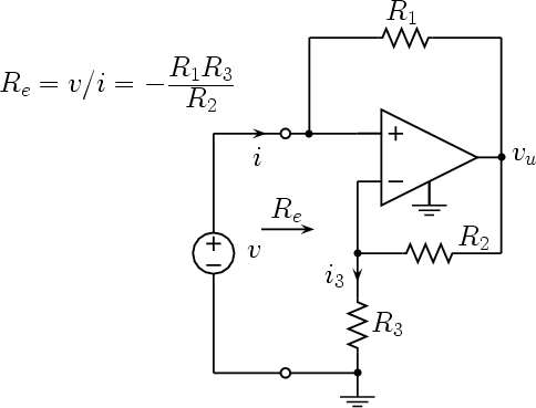
The circuit used is shown in Fig. 6. Its input resistance Re is given by the ratio v/i. To evaluate Re, let us first observe that, due to the constraints imposed by the op amp, the voltage of the inverting input (with respect to ground) is v. Hence

and

Since

we have

and hence

If we set R1 = R2 we get

The above equations are valid as far as the op amp works in its linear region, that is as far as |vu| < Es, being Es (Es > 0) the saturation voltage of the op amp. Taking into account the expression of vu, the op amp works in its linear region as long as

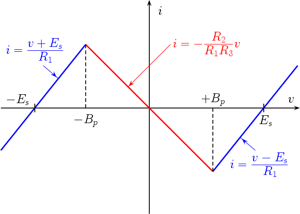
The breakpoint voltages of the v ÷ i characteristic are symmetric with respect to the origin and the positive one, Bp, is given by

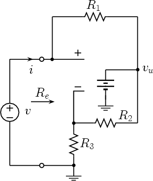
When v > Bp the op amp enters its positive saturation region. The equivalent circuit is given in Fig. 7 and the expression of i becomes

A similar reasoning holds when v < -Bp: in this case the op amp enters its negative saturation region and now the expression of i becomes

The whole characteristic is shown in Fig. 8
2.3 Design formulas of the piecewise resistor
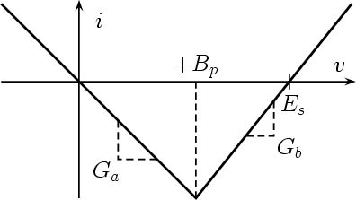
According to the results of the previous section and assuming that the saturation voltage Es of the op amp is known, the inner slope Ga, the outer slope Gb, and the breakpoint voltage Bp (see Fig. 9) are given by

Now let us suppose that the inner slope Ga (Ga < 0) , the outer slope Gb, and the value of the breakpoint voltage Bp are assigned. The design formulas can be obtained from the equations above. If we assume R1 = R2, from the first two equations we get

The third equation links the breakpoint voltage Bp to the saturation voltage Es. Note that Es is assumed known and fixed at a particular value, that depends on the internal structure of the op amp and on the used power supply voltages. It is not known a priori but it can be measured. As a consequence, it turns out that the value of Bp cannot be fixed independently from the ratio Ga/Gb (even if R2 is not chosen equal to R1).

or, equivalently

Finally, it is worth noting to observe that the above equation also states the continuity of the characteristic at the breakpoint Bp.
2.4 The Chua’s diode
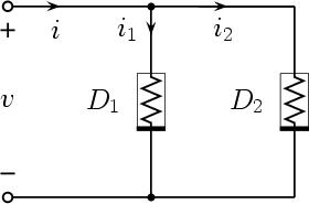
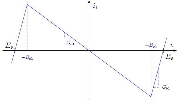
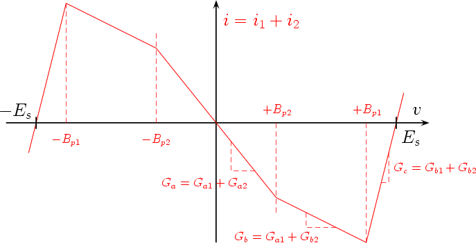
The Chua’s diode can be obtained by the parallel connection of two piecewise nonlinear resistors of the kind described in the previous Subsection, as shown in Fig. 10. Since the voltage v across the two resistors D1 and D2 is the same, the resulting characteristic is obtained by summing the currents i1 and i2 for equal values of v, as shown in Fig. 11
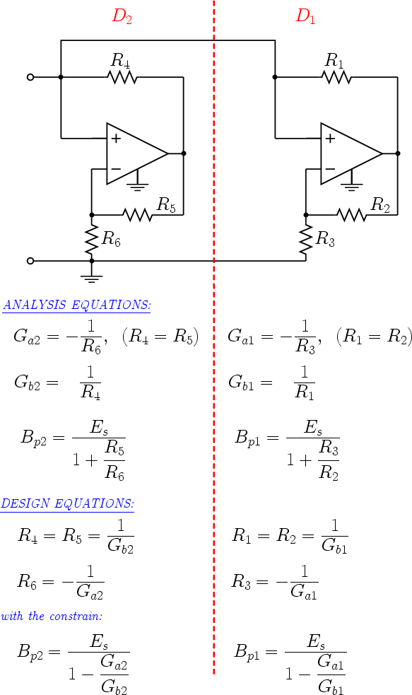
The complete circuit is shown in Fig. 12, along with the analysis and design equations for each diode.
2.5 Evaluation of the design parameters
Referring to Fig. 11, the shape of the desired characteristic is determined by Ga, Gb, Bp2, and Bp1. The value of Bp1 only influences the extension of the negative-slope region and, hence, it is less relevant for the final design. Furthermore, the saturation voltage Es is supposed to be known and equal for both the op amps.
To design the Chua’s diode, we must first compute the values of the slopes Ga1 , Gb1 , Ga2 , and Gb2 of the two diodes D1 and D2 . First, from Fig. 11 we obtain the following two equations

Furthermore, the following two constraints (see Fig. 12) hold

Altogether, we obtain the following system of four equations in the four unknown Ga1 , Gb1 , Ga2 , and Gb2

Since Gb1 does not appear in the first three equations of the system, they can be solved independently from the fourth equation. We obtain

Solving this system we obtain
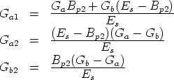
and, from the fourth equation

Using the design equations listed in Fig. 12 it is now possible to compute the element values of the Chua’s diode, as explained in the following Subsection.
2.6 Design procedure
We are now able to suggest a design procedure for the Chua’s diode. Once again we would like to stress that the value of Bp1 is not critical and it only should be large enough to ensure that the dynamics of the attractor remains within the negative-resistance region of the whole characteristic. Then the design procedure can follow these five steps
- Choose

- Evaluate

- Evaluate

- Evaluate

Note that this value is generally high, since the difference Gb - Ga is typically small, and hence the resistors R4 and R5 do not load significantly the op amp.
- Evaluate

If the obtained value of R1 (and R2) is too small and loads the op amp, we can assign smaller values to Bp1 until a trade off is reached between the length of the negative-resistance region and the size of R1. Generally, to use off-the-shelf components, one assigns a suitable value to R1 and then evaluates Bp1

If this value is too small, then a new (smaller) value of R1 is used.
2.7 An example
Assume that the op amps are powered by two 9 V batteries and that the saturation voltage equals 8.3 V . The required slopes in the negative-resistance region - capable to assure interesting dynamic behaviors - are chosen to be Ga = -0.756 mS and Gb = -0.409 mS. The inner-breakpoint value is set to Bp2 = 1.08 V . According to the outlined procedure we get

After some trials, we chose

The value of the breakpoint Bp1 turns out to be high enough, compared to a saturation voltage of 8.3 V

3 Designing the Chua’s oscillator
To complete the realization of a Chua’s oscillator, we have still to chose the values of the two capacitors C1, C2, and of the inductor L. The resistor R0 can be assumed equal to the measured leakage resistor which models the loss of the real inductor L, whereas the resistor R is used as bifurcation parameter and hence it is varied in a quite wide range of values. Furthermore, we have to fix the characteristic of the Chua’s diode, that is the values of Ga, Gb, Bp2, and (less critical) of Bp1.
All these values should be fixed in such a way that an interesting dynamic behavior is obtained as R is varied and, possibly, the circuit elements have suitable values, so that off-the-shelf components can be used.
In the first reported study [1] of the classical Chua’s circuit (i.e. a Chua’s oscillator with R0 =  = 0),
a strange attractor is obtained by simulating a system of differential equations using the following set of
(scaled) component values:


These values correspond to the following set of dimensionless parameters:

Even if the Chua’s oscillator is considered (with small values of  , i.e. of R0), extended simulations show
that interesting dynamical behaviors are still observed if similar dimensionless parameter values are used.
To use standard component values, we arbitrarily choose C2 = 100 nF and C1 = 10 nF, that corresponds
to
  = 10. Furthermore, we choose L = 18 mH and the variable resistor R in the range of 2 k
 , that
approximately corresponds to the value of
  used in [1].
Finally, we use slightly different values for Ga, Gb and Bp2 in order to get standard resistor values for the Chua’s diode. The value of Bp1 is less critical: it is not fixed “a priori” and is accepted as long as it is sufficiently high, as explained in the previous Section.
The choice of these values is in part related to the op amp saturation voltage and is generally done in an heuristic way. For example, in a real circuit where two 9 V batteries are used to power the op amps, the (measured) saturation voltage equals 8.3 V . In this case, after a few trials, we get suitable component values (see Subsection 2.7) assuming Ga = -0.756 mS, Gb = -0.409 mS and setting the inner-breakpoint Bp2 to 1.08 V .
The complete list of the circuit components is given in Tab. 1
|
References
